Please submit your message online, we will contact you as soon as possible!

Author:A
Silicon through hole technology can be divided into two categories according to the literal meaning and the filling method of electroplated copper: one is TSV copper plating with small Aspect Ratio and equal wall growth of hole copper, such as image sensor and fingerprint recognition chip packaging mostly in accordance with this method; The other is Super Filling (TSV) electroplated copper, represented by MEMS, etc. The TSV packaging process of CIS (CMOS Image Sensor) is a silicon through hole process belonging to the narrow concept of TSV. Through silicon perforation, the upper and lower lines are connected to achieve the purpose, and it has not risen to the height of 3D integration, which is different from the concept of TSV system integration mentioned by SiP in the industry. But CIS encapsulation is an important part of the sealing process at present, this paper will be included in the TSV category to explain.
An image sensor is a device that converts optical signals into electrical signals. There are two main types of image sensing chips: CCD and CMOS, the former is composed of optocouplers, the latter is composed of metal oxide devices. Compared with CCD, CMOS image sensor has a fast frame display rate, a high degree of integration (can reduce the use of peripheral components, reduce system costs), and low power consumption and other characteristics, and CIS is a standard process, in terms of manufacturing costs, product prices have obvious advantages, so CIS in recent years in the camera mobile phone applications have been rapid development. Since March 2007, Toshiba Corporation of Japan has adopted TSV technology for the first time in the wafer-level package of small image sensor modules, this technology continues to attract the world's major image sensor manufacturers have invested in the ranks of TSV photographic modules. In 2008, global CIS shipments exceeded CCD image sensor shipments for the first time. In recent years, with the development of CIS technology, the proportion of CCD technology in the market has declined significantly. CMOS image sensor (CIS) is the integration of analog circuit and digital circuit, mainly composed of four components: microlens, color filter (CF), photodiode (PD), pixel design.
The booming development of image sensors, mostly benefited from the Camera Phone (Camera Phone). The mobile phone has moved from the "mobile phone" with the single function of making calls and sending messages to the multimedia function, which can meet the needs of music, video, Internet, photography, office and entertainment. In 2000, Sharp launched the first mobile phone that can take pictures, followed by the arrival of the smartphone era, the main camera pixels continue to improve, and the camera has moved from single to dual and multi-camera. Despite the downturn in smartphone sales in 2019, sales of mobile phone image sensors grew by about 20%. In addition, with the rise of the security monitoring market, the global automotive electronics, medical devices, and military fields have also created considerable application scale for image sensors, and the demand for image sensors will continue to rise. CMOS image sensors grew 20% year on year in 2017, the global CIS market size was $15.5 billion in 2018, and is expected to grow 10% in 2020 to reach $17 billion. In view of the rapid development of image sensors, the TSV packaging process used by its chips (as opposed to the traditional Bumping process) will become an important part of the packaging industry. At present, several domestic enterprises represented by Huatian Technology have the mass production capacity of CIS packaging process.
The chemical nickel-gold process shown in this process (see below) is an important structure of Under-Bump Metallization (UBM). Chemical nickel-gold or nickel-palladium processes are not only for CIS packaging. Generally used as wire, solder or tin ball base UBM can use chemical nickel (palladium) gold to improve reliability. The nickel layer is a barrier layer, which can prevent the diffusion of aluminum or copper substrate and solder or gold wire; The palladium layer has a dual function, not only as a barrier layer to further reduce diffusion, but also has a good bonding function. The gold layer has good antioxidant capacity and good wiring function. Chemical nickel gold or nickel palladium refers to a layer of 2 to 5 microns of nickel is first deposited on the copper or aluminum based UBM pad after multiple pre-treatment, and then a layer of palladium is deposited on the surface of palladium. For general products, the use of nickel gold structure can meet the requirements, for products with high reliability requirements, it is recommended to use chemical nickel palladium structure. When applied to lead-free solder (SAC 305 solder paste) welding, the thickness of chemical nickel palladium is 0.05 ~ 0.1 micron for palladium layer and 0.05 ~ 0.1 micron for gold layer. When applied to wire bonding, the thickness of chemical nickel palladium is 0.1 to 0.2 microns for palladium layer, 0.1 to 0.2 microns for gold layer (quality priority) or 0.05 to 0.1 microns for gold layer (cost consideration).
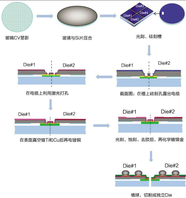
CIS packaging process flow diagram
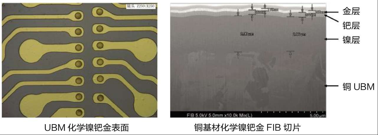
镍钯金化学镀示例图
Nickel palladium gold electroless plating example
For a long time, chemical gold plating often uses potassium aurous cyanide as the main salt, with the increasingly stringent environmental requirements, the industry began to use cyanide-free gold instead of cyanide gold plating, and has a mature market application case. Compared with electroplating, electroless plating has obvious advantages. Electroless plating has lower requirements on equipment, low concentration of gold tank opening and good uniformity of coating, which can save gold salt and reduce cost. In addition, the electroless plating production efficiency is higher, and the electroless plating area can be an independent pad, which is not restricted by the graphic circuit. Because electroless plating has the advantage of low investment, some people have tried to use electroless copper plating to replace vacuum copper plating in recent years.
If you are interested in this article, please immediatelycontact us

Support Hotline
Please submit your message online, we will contact you as soon as possible!