请在线提交您的留言,我们将尽快联系您!

作者:YU YAO
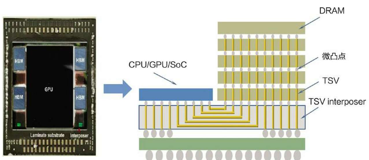
SiP technology was proposed in the 1990s, has been accepted and flourished in the industry for more than 20 years, and still has a large space for development in the foreseeable future. SiP is a system integration engineering problem, due to the integration of multi-chip, in the design must consider electrical, thermal and mechanical mechanics and other aspects, to make more reliable design, choose the right material and the best process, but also consider the cycle, cost, supply chain and risk control and other factors. Due to different product applications and needs, SiP design and manufacturing has no fixed model, each manufacturer has its own set of processes, different product processes will also be different. The initial SiP mainly designed the multi-chip distributed structure on a two-dimensional plane, and realized integration through the carrier board. Although the definition of SiP was realized, it was still relatively unable to meet the needs of high-end electronic products in the consumer market in terms of technical indicators such as volume, operating efficiency and power consumption. With the continuous development of chip packaging technology, some chips from two-dimensional planar distribution arrangement to three-dimensional stacking mode, which is currently a more advanced SiP mode, we can call it 2.5D SiP process. It can be expected that the multi-chip 3D overlay SiP technology will further shorten the line distance of interconnection and further improve the integration, which is also the final development goal of 3D SiP.

2.5D 封装工艺示意图

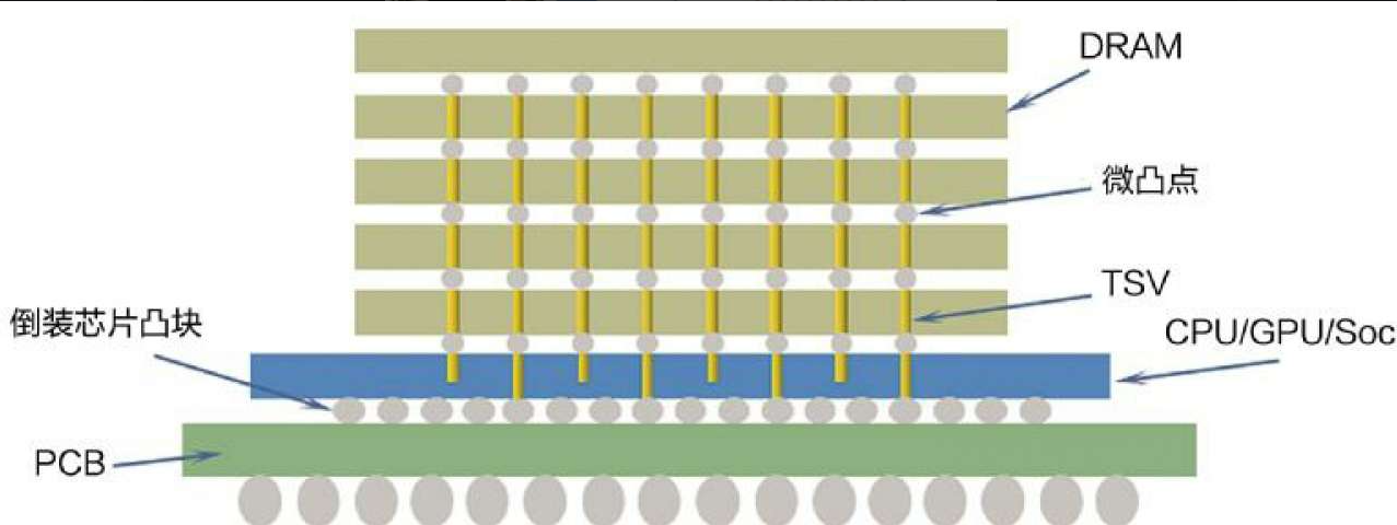
3D 封装工艺示意图
Compare the above two figures to understand the difference between 2.5D and 3D packaging. The 3D package will stack the CPU/GPU/SoC and DRAM and connect and integrate in the vertical direction, and the area of the package is smaller than the 2.5D package process, and the TSV interposer is also removed from the 2.5D package.
如果您对这篇文章感兴趣,请立即联系我们
请在线提交您的留言,我们将尽快联系您!